
Introduction
In the information society, people receive a large amount of information each day. As the main interface facilitating exchange between people and information, display products have a significant impact on people’s lives. Given the rapid increase of information—in particular the replacement of traditional single text video information by the multimedia digital audio —higher demand of display quality and resolutuion is proposed for the display device. Therefore, various new display technologies are booming, especially the new generation of display technology, Micro LED, which has become a technical highland for display manufacturers. In response to this shift, Absen released the Micro LED display technology worldwide on 12 March 2021.
1 Comparison of mainstream display technologies
Different scenarios propose different performance requirements for display device s, and the corresponding mainstream display technologies selected are also different . According to usage scenarios, display devices can be divided into 2C display and 2B display.
2C display mainly refers to TVs, monitors, laptops, in-vehicle products, mobile phones, wearable products etc. LCD is the traditional technical solution mainly applied to 2C display, while it suffers from issues such as low contrast, small color gamut and limited viewing angle. With the development of material technologies, OLED technology has emerged. Compared with LCD, OLED boasts significant advantages including simpler frames, thinner overall thickness, higher brightness and contrast, larger viewing angle, wider color gamut range and lower power consumption. These strengths have quickly enabled OLED display products to dominate the consumer market. However, OLED display products also have disadvantages such as short life. Micro LED is characterized by display technology that minimizes the LED display to a micron scale, which matches the long life and reliability of inorganic LED. This technology results in displays that feature high brightness, high contrast, wide color gamut, long service life and high reliability. Due to these qualities, the micro LED display is considered to be a near perfect display technology. The high brightness and energy-saving capabilities favor broad application prospects of micro LED in 0.x-inch and x-inch wearable products, while Apple, as a representative, expects to apply Micro LED technology to 2C products such as the Apple Watch. On the other hand, the advantage of seamless splicing renders the Micro LED the best solution for large screen TV products above 85-inch. Currently, Sony, Samsung and some domestic display manufacturers have launched large screen consumer products based on Micro LED technology.
2B display
mainly refer
s to outdoor
and indoor
large screens
in the
theaters, shopping malls, meeting rooms, control rooms, etc. The mainstream display technologies selected for these use scenarios include LCD splicing display, projection display and LED large screen display.
The imposssibility of
seamless splicing
for LCD and the
poor brightness
and
contrast
for
projection display
limit
their
application
, while
LED display characterized by high brightness, high contrast, wide color gamut, available seamless splicing and other advantages
becomes the most promising display technology
.
With the decrease of dot pitch, especially the development of Micro LED technology, the ultra-high definition of LED display has become a trend,
and
the display quality is getting more and more delicate
.
Consequently
,
the application scenarios
for LED
display are also expanding from the traditional engineering
d
isplay
to the commercial display and
i
n-
h
ome
d
isplay
.
It can be seen that Micro LED is highly competitive in both 2C and 2B markets because of its unique advantages
. Accordingly, both t
raditional panel manufacturers and LED display manufacturers are actively d
evelop
ing this technology. As a global leading supplier for true LED display applications and services
,
Absen is no exception.
At present, Absen has launched the following Micro LED commercial display products worldwide: 2K 55-inch (P0.6), 2K 73-inch (P0.8), 2K 82-inch (P0.9), 4K 110-inch (P0.6), 4K 138-inch (P0.7), 4K 165-inch (P0.9) and 8K 220-inch (P0.6).
Micro LED display technology can be deemed as the micro pitch and HD of traditional LED displays
, and t
iny LED particles
are used as the
pixel light-emitting points
. Accordingly, the
structure and encapsulation
of
LED chip
directly affect the performance of Micro LED display devices.
2 Structural comparison of Micro LED light emitting chips
Generally, the LED chip is composed of the substrate, P-type semiconductor layer, N-type semiconductor layer, P-N junction , positive electrode and negative electrode. When the positive voltage is applied between the positive electrode and negative electrode, the holes injected from the P area to the N area and the electrons injected from the N area to the P area recombine at the PN junction, converting the electrical energy into light with different wavelength . The structure of LED chips is mainly divided into the following types : wire-bonding structure , flip structure and vertical structure . Figure 1 shows the schematic design of three chip structures.
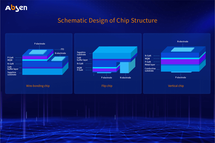
Figure 1 Schematic Design of Chip Structure
(1) Structure of wire-bonding chip
As the earliest chip structure , the wire-bonding chip is composed of the following from top to bottom: electrodes, P-type semiconductor layer, light emitting layer, N-type semiconductor layer and substrates.In this structure, t he heat generated at the PN junction in this structure needs to pass through the sapphire substrate to be conducted to the heat sink . T he poor thermal conductivity of the sapphire leads to poor thermal conductivity of the structure, thereby reducing the luminous efficiency and reliability of the chip . In the structure of the wire-bonding chip, the p-electrode and n-electrode are both located on the light-emitting surface of the chip, and the shielding of the electrodes will resul t in low luminous efficiency of the chip . Furthermore, locating the p-electrode and n-electrode on the same side of the chip is also prone to current crowding, which will reduce the luminous efficiency. Additionally, electrode metal drift may be caused by factors such as temperature, humidity and etc , which will result in short-circuit problems as the reduction of the chip size and the distance between positive and negative electrode s.
(2) Structure of flip chip
The flip chip is composed of the following from top to bottom: sapphire substrate, N-type semiconductor layer, light emitting layer, P-type semiconductor layer and electrodes. Compared with the wire-bonding chip, the heat generated at the P-N junction of this structure can be directly conducted to the heat sink without passing through the substrate , resulting in excellent heat dissipation performance and thus excellent luminous efficiency and reliability. I n the flip structure, both p electrode and n electrode are located on the bottom, which avoids the obstruction of light emitted from the top and contribute s to a high light output efficiency . Additionally , the long distance between positive and negative electrode s in the flip structure can reduce the risk of short circuit caused by metal migration of the electrodes.
(3) Structure of vertical chip
Different from the the wire-bonding chip, the substrate with high thermal conductivity (Si, Ge or Cu substrate) instead of sapphire substrate is used in the vertical chip , which greatly improves the heat dissipation performance of the chip. Moreover , the positive electrode and negative electrode of the vertical chip are located on the top and bottom of the chip separately , which contributes to more uniform distribution of the current and heat and further improve d reliability of the chip. At the present however, the current vertical chip suffers from high cost and low mass production capacity .
Table 1 outlines the performance comparison of these three chips. It can be seen that the flip chip is more suitable for
micro LED
display products
due to the high luminous efficiency, good heat dissipation
performance
, high reliability and mass production
capacity.
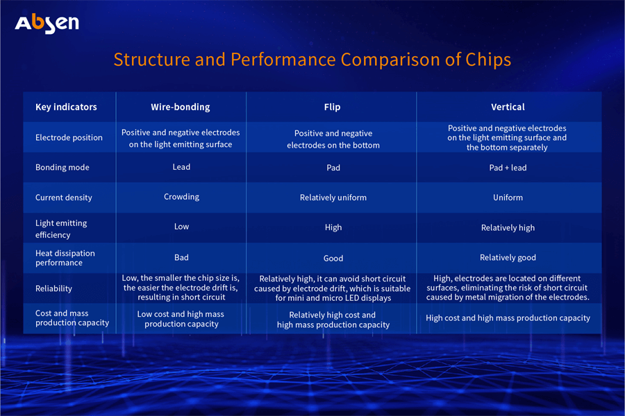
Table 1 Structure and Performance Comparison of Chips
3 Comparison of
the e
ncapsulation
forms of
Micro LED
Bare
LED chip
without encapsulation
cannot meet the requirements
of use and
thus
reasonable
encapsulation
should be
designed to
provid
e
electrical
connection
, mechanical protection, effective heat dissipation channels
and
high-efficiency and high-quality light output.
The reduction of LED chip size and display screen pitch put
s
forward higher requirements for encapsulation. At present, Chip-type SMD , N-in-one IMD and COB
are
the commonly used
encapsulation
forms
, as shown in Figure 2.
Figure 2 Schematic Design of Typical Micro LED Encapsulation Structures
(1) Chip-type SMD encapsulation
In Chip-type SMD encapsulation , a single LED pixel is die bonded on the BT board and then encapsulated using the optical resin to achieve a single Chip-type encapsulation . The Chip-type encapsulation is then a ttached on the PCB using SMD technology to create the LED display module to obtain the LED display module . Chip-type SMD encapsulation is a single pixel encapsulation with small size, small solder joint area and plenty of solder joints , which will result in the risks of water vapor erosion, poor m echanical protection and short circuit . Based on the above analysis , Chip-type SMD encapsulation is not suitable for Micro LED displays.
(2) N-in-one IMD encapsulation
In N-in-one IMD encapsulation , N pixel units (mostly 2 or 4) are die bonded on the BT board and then encapsulated as a whole using the optical resin. C ompared with Chip-type SMD encapsulation , IMD encapsulation boasts higher integration, which can effectively relieve risks of water vapor erosion and poor m echanical protection . Meanwhile, IMD encapsulation inherits the advantages of mature process, low technical difficulty and cost of the single SMD device . However, the integration of N-in-one IMD encapsulation is still low , resulting in issues of process, display effect and reliability for micro pitch displays below 0.6mm.
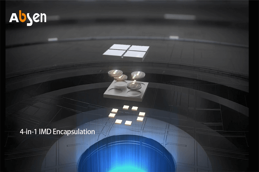
IMD 4-in-1
Integrated encapsulation technology
(3) COB encapsulation
In COB encapsulatiuon, naked chips of multiple pixel units(mostly hundreds ) are die bonded on the PCB and then encapsulated as a whole using the optical resin. C ompared with Chip-type SMD encapsulation and N-in-one IMD encapsulation, multiple chips are encapsulated as a whole in the COB encapsulatiuon, which contributes to improved resistance to water vapor and excellent mechanical protection performance. Moreover, BT board is omitted and the naked LED chips are a ttached on the PCB directly in COB encapsulatiuon , which provide s a shorter heat conduction channel and thus better heat dissipation performance . From the above analysis, it can be demonstrated that COB encapsulatiuon is the optimum form for Micro LED displays with high pixel density.
The characteristics of the abovementioned encapsulation methods are shown in Table 2. COB encapsulation
with the highest degree of integration can be used to achieve the smallest pixel pitch, the highest reliability and the longest display life theoretically and is thought to be the best packaging solution for Micro LED.
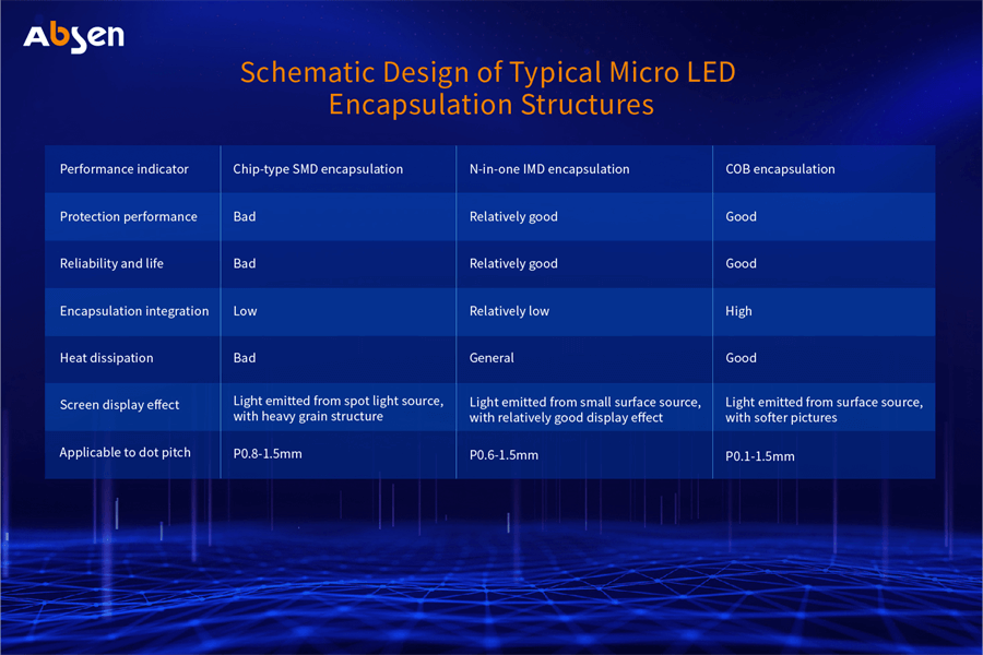
Table 2 Comparison of Encapsulation Method and Performance of Micro LED Display Products
4 Conclusion
Micro LED is considered to be a nearly perfect display technology and has broad application prospects in the field of large-screen displays above 85 inches because of its advantages of high brightness, high contrast, wide color gamut, and seamless splicing. Major display manufacturers are actively deploying in the Micro LED display field. T he structure and encapsulation of LED chip directly determine the performance of Micro LED display devices. At present, three kinds of structure, namely the wire-bonding structure, flip structure and vertical structure, are mainly adopted in the industry. It can be seen from the comparison of those structures that the flip chip with high light emitting efficiency, good heat dissipation performance, high reliability and high mass production capacity is more suitable for Micro LED displays. Typically, Micro LED encapsulation forms include Chip-type SMD encapsulation, N-in-one IMD encapsulation and COB encapsulation. Among these three kinds of encapsulation, COB encapsulation with the highest integration can be used to achieve the smallest pixel pitch, the highest reliability and the longest display life theoretically and is thought to be the best packaging solution for Micro LED.
The full range of Micro LED products released by Absen are based on Absen proprietary HCCI technology.
1) Use the flip chip COB encapsulation technology
2) Integrate Absen’s core algorithm HDR3.0
3) Integrate the intelligent display technology
A professional team has been continuously researching on
the
optical design
and
image quality processing
to improve the
display effect.
These efforts have
contributed to
smooth images, high color reproduction,
gentle
and
consistent
display. All the
results have been applied to products
which
are widely used in scenarios such as large control centers and conference centers.
 简体中文 / 中国
 Japanese / 日本
 English / Europe
 русский / Russian
 Español / Spanish
 Español / Mexico
 Português / Brazil